Showing posts with label Digital. Show all posts

DIGITAL STORAGE (MEMORY)

Why digital?

Although many textbooks provide good introductions to digital memory technology, I intend to make this chapter unique in presenting both past and present technologies to some degree of detail. While many of these memory designs are obsolete, their foundational principles are still quite interesting and educational, and may even find re-application in the memory technologies of the future.

The basic goal of digital memory is to provide a means to store and access binary data: sequences of 1's and 0's. The digital storage of information holds advantages over analog techniques much the same as digital communication of information holds advantages over analog communication. This is not to say that digital data storage is unequivocally superior to analog, but it does address some of the more common problems associated with analog techniques and thus finds immense popularity in both consumer and industrial applications. Digital data storage also complements digital computation technology well, and thus finds natural application in the world of computers.

The most evident advantage of digital data storage is the resistance to corruption. Suppose that we were going to store a piece of data regarding the magnitude of a voltage signal by means of magnetizing a small chunk of magnetic material. Since many magnetic materials retain their strength of magnetization very well over time, this would be a logical media candidate for long-term storage of this particular data (in fact, this is precisely how audio and video tape technology works: thin plastic tape is impregnated with particles of iron-oxide material, which can be magnetized or demagnetized via the application of a magnetic field from an electromagnet coil. The data is then retrieved from the tape by moving the magnetized tape past another coil of wire, the magnetized spots on the tape inducing voltage in that coil, reproducing the voltage waveform initially used to magnetize the tape).

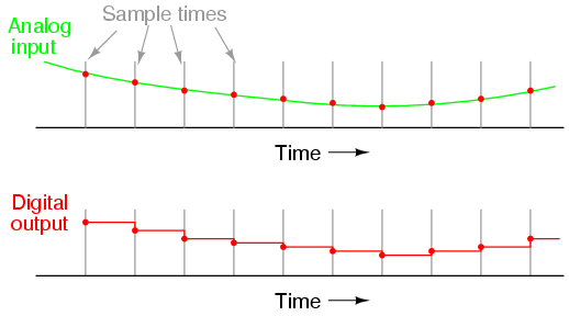
If we represent an analog signal by the strength of magnetization on spots of the tape, the storage of data on the tape will be susceptible to the smallest degree of degradation of that magnetization. As the tape ages and the magnetization fades, the analog signal magnitude represented on the tape will appear to be less than what it was when we first recorded the data. Also, if any spurious magnetic fields happen to alter the magnetization on the tape, even if its only by a small amount, that altering of field strength will be interpreted upon re-play as an altering (or corruption) of the signal that was recorded. Since analog signals have infinite resolution, the smallest degree of change will have an impact on the integrity of the data storage.

If we were to use that same tape and store the data in binary digital form, however, the strength of magnetization on the tape would fall into two discrete levels: "high" and "low," with no valid in-between states. As the tape aged or was exposed to spurious magnetic fields, those same locations on the tape would experience slight alteration of magnetic field strength, but unless the alterations were extreme, no data corruption would occur upon re-play of the tape. By reducing the resolution of the signal impressed upon the magnetic tape, we've gained significant immunity to the kind of degradation and "noise" typically plaguing stored analog data. On the other hand, our data resolution would be limited to the scanning rate and the number of bits output by the A/D converter which interpreted the original analog signal, so the reproduction wouldn't necessarily be "better" than with analog, merely more rugged. With the advanced technology of modern A/D's, though, the tradeoff is acceptable for most applications.

Also, by encoding different types of data into specific binary number schemes, digital storage allows us to archive a wide variety of information that is often difficult to encode in analog form. Text, for example, is represented quite easily with the binary ASCII code, seven bits for each character, including punctuation marks, spaces, and carriage returns. A wider range of text is encoded using the Unicode standard, in like manner. Any kind of numerical data can be represented using binary notation on digital media, and any kind of information that can be encoded in numerical form (which almost any kind can!) is storable, too. Techniques such as parity and checksum error detection can be employed to further guard against data corruption, in ways that analog does not lend itself to.


Digital memory terms and concepts

When we store information in some kind of circuit or device, we not only need some way to store and retrieve it, but also to locate precisely where in the device that it is. Most, if not all, memory devices can be thought of as a series of mail boxes, folders in a file cabinet, or some other metaphor where information can be located in a variety of places. When we refer to the actual information being stored in the memory device, we usually refer to it as the data. The location of this data within the storage device is typically called the address, in a manner reminiscent of the postal service.

With some types of memory devices, the address in which certain data is stored can be called up by means of parallel data lines in a digital circuit (we'll discuss this in more detail later in this lesson). With other types of devices, data is addressed in terms of an actual physical location on the surface of some type of media (the tracks and sectors of circular computer disks, for instance). However, some memory devices such as magnetic tapes have a one-dimensional type of data addressing: if you want to play your favorite song in the middle of a cassette tape album, you have to fast-forward to that spot in the tape, arriving at the proper spot by means of trial-and-error, judging the approximate area by means of a counter that keeps track of tape position, and/or by the amount of time it takes to get there from the beginning of the tape. The access of data from a storage device falls roughly into two categories: random access and sequential access. Random access means that you can quickly and precisely address a specific data location within the device, and non-random simply means that you cannot. A vinyl record platter is an example of a random-access device: to skip to any song, you just position the stylus arm at whatever location on the record that you want (compact audio disks so the same thing, only they do it automatically for you). Cassette tape, on the other hand, is sequential. You have to wait to go past the other songs in sequence before you can access or address the song that you want to skip to.

The process of storing a piece of data to a memory device is called writing, and the process of retrieving data is called reading. Memory devices allowing both reading and writing are equipped with a way to distinguish between the two tasks, so that no mistake is made by the user (writing new information to a device when all you wanted to do is see what was stored there). Some devices do not allow for the writing of new data, and are purchased "pre-written" from the manufacturer. Such is the case for vinyl records and compact audio disks, and this is typically referred to in the digital world as read-only memory, or ROM. Cassette audio and video tape, on the other hand, can be re-recorded (re-written) or purchased blank and recorded fresh by the user. This is often called read-write memory.

Another distinction to be made for any particular memory technology is its volatility, or data storage permanence without power. Many electronic memory devices store binary data by means of circuits that are either latched in a "high" or "low" state, and this latching effect holds only as long as electric power is maintained to those circuits. Such memory would be properly referred to as volatile. Storage media such as magnetized disk or tape is nonvolatile, because no source of power is needed to maintain data storage. This is often confusing for new students of computer technology, because the volatile electronic memory typically used for the construction of computer devices is commonly and distinctly referred to as RAM (Random Access Memory). While RAM memory is typically randomly-accessed, so is virtually every other kind of memory device in the computer! What "RAM" really refers to is the volatility of the memory, and not its mode of access. Nonvolatile memory integrated circuits in personal computers are commonly (and properly) referred to as ROM (Read-Only Memory), but their data contents are accessed randomly, just like the volatile memory circuits!

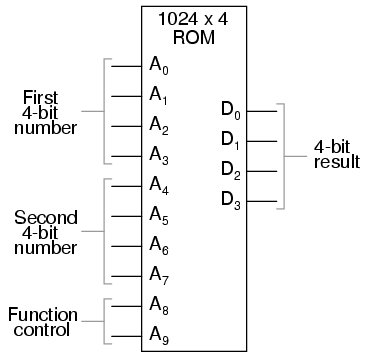
Finally, there needs to be a way to denote how much data can be stored by any particular memory device. This, fortunately for us, is very simple and straightforward: just count up the number of bits (or bytes, 1 byte = 8 bits) of total data storage space. Due to the high capacity of modern data storage devices, metric prefixes are generally affixed to the unit of bytes in order to represent storage space: 1.6 Gigabytes is equal to 1.6 billion bytes, or 12.8 billion bits, of data storage capacity. The only caveat here is to be aware of rounded numbers. Because the storage mechanisms of many random-access memory devices are typically arranged so that the number of "cells" in which bits of data can be stored appears in binary progression (powers of 2), a "one kilobyte" memory device most likely contains 1024 (2 to the power of 10) locations for data bytes rather than exactly 1000. A "64 kbyte" memory device actually holds 65,536 bytes of data (2 to the 16th power), and should probably be called a "66 Kbyte" device to be more precise. When we round numbers in our base-10 system, we fall out of step with the round equivalents in the base-2 system.

Modern nonmechanical memory

Now we can proceed to studying specific types of digital storage devices. To start, I want to explore some of the technologies which do not require any moving parts. These are not necessarily the newest technologies, as one might suspect, although they will most likely replace moving-part technologies in the future.

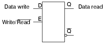
A very simple type of electronic memory is the bistable multivibrator. Capable of storing a single bit of data, it is volatile (requiring power to maintain its memory) and very fast. The D-latch is probably the simplest implementation of a bistable multivibrator for memory usage, the D input serving as the data "write" input, the Q output serving as the "read" output, and the enable input serving as the read/write control line:

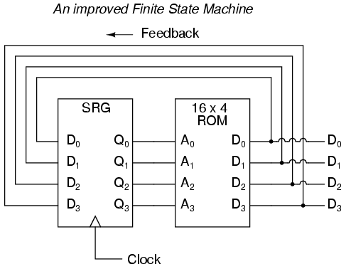
If we desire more than one bit's worth of storage (and we probably do), we'll have to have many latches arranged in some kind of an array where we can selectively address which one (or which set) we're reading from or writing to. Using a pair of tristate buffers, we can connect both the data write input and the data read output to a common data bus line, and enable those buffers to either connect the Q output to the data line (READ), connect the D input to the data line (WRITE), or keep both buffers in the High-Z state to disconnect D and Q from the data line (unaddressed mode). One memory "cell" would look like this, internally:

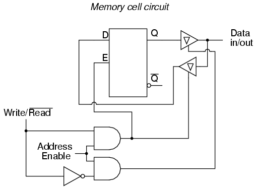
When the address enable input is 0, both tristate buffers will be placed in high-Z mode, and the latch will be disconnected from the data input/output (bus) line. Only when the address enable input is active (1) will the latch be connected to the data bus. Every latch circuit, of course, will be enabled with a different "address enable" (AE) input line, which will come from a 1-of-n output decoder:

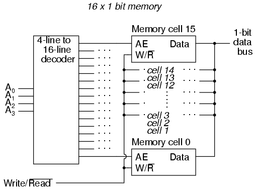
In the above circuit, 16 memory cells are individually addressed with a 4-bit binary code input into the decoder. If a cell is not addressed, it will be disconnected from the 1-bit data bus by its internal tristate buffers: consequently, data cannot be either written or read through the bus to or from that cell. Only the cell circuit that is addressed by the 4-bit decoder input will be accessible through the data bus.

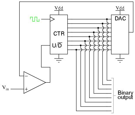
This simple memory circuit is random-access and volatile. Technically, it is known as a static RAM. Its total memory capacity is 16 bits. Since it contains 16 addresses and has a data bus that is 1 bit wide, it would be designated as a 16 x 1 bit static RAM circuit. As you can see, it takes an incredible number of gates (and multiple transistors per gate!) to construct a practical static RAM circuit. This makes the static RAM a relatively low-density device, with less capacity than most other types of RAM technology per unit IC chip space. Because each cell circuit consumes a certain amount of power, the overall power consumption for a large array of cells can be quite high. Early static RAM banks in personal computers consumed a fair amount of power and generated a lot of heat, too. CMOS IC technology has made it possible to lower the specific power consumption of static RAM circuits, but low storage density is still an issue.

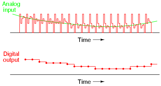
To address this, engineers turned to the capacitor instead of the bistable multivibrator as a means of storing binary data. A tiny capacitor could serve as a memory cell, complete with a single MOSFET transistor for connecting it to the data bus for charging (writing a 1), discharging (writing a 0), or reading. Unfortunately, such tiny capacitors have very small capacitances, and their charge tends to "leak" away through any circuit impedances quite rapidly. To combat this tendency, engineers designed circuits internal to the RAM memory chip which would periodically read all cells and recharge (or "refresh") the capacitors as needed. Although this added to the complexity of the circuit, it still required far less componentry than a RAM built of multivibrators. They called this type of memory circuit a dynamic RAM, because of its need of periodic refreshing.

Recent advances in IC chip manufacturing has led to the introduction of flash memory, which works on a capacitive storage principle like the dynamic RAM, but uses the insulated gate of a MOSFET as the capacitor itself.

Before the advent of transistors (especially the MOSFET), engineers had to implement digital circuitry with gates constructed from vacuum tubes. As you can imagine, the enormous comparative size and power consumption of a vacuum tube as compared to a transistor made memory circuits like static and dynamic RAM a practical impossibility. Other, rather ingenious, techniques to store digital data without the use of moving parts were developed.

Historical, nonmechanical memory technologies

Perhaps the most ingenious technique was that of the delay line. A delay line is any kind of device which delays the propagation of a pulse or wave signal. If you've ever heard a sound echo back and forth through a canyon or cave, you've experienced an audio delay line: the noise wave travels at the speed of sound, bouncing off of walls and reversing direction of travel. The delay line "stores" data on a very temporary basis if the signal is not strengthened periodically, but the very fact that it stores data at all is a phenomenon exploitable for memory technology.

Early computer delay lines used long tubes filled with liquid mercury, which was used as the physical medium through which sound waves traveled along the length of the tube. An electrical/sound transducer was mounted at each end, one to create sound waves from electrical impulses, and the other to generate electrical impulses from sound waves. A stream of serial binary data was sent to the transmitting transducer as a voltage signal. The sequence of sound waves would travel from left to right through the mercury in the tube and be received by the transducer at the other end. The receiving transducer would receive the pulses in the same order as they were transmitted:

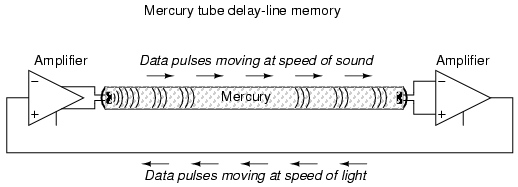
A feedback circuit connected to the receiving transducer would drive the transmitting transducer again, sending the same sequence of pulses through the tube as sound waves, storing the data as long as the feedback circuit continued to function. The delay line functioned like a first-in-first-out (FIFO) shift register, and external feedback turned that shift register behavior into a ring counter, cycling the bits around indefinitely.

The delay line concept suffered numerous limitations from the materials and technology that were then available. The EDVAC computer of the early 1950's used 128 mercury-filled tubes, each one about 5 feet long and storing a maximum of 384 bits. Temperature changes would affect the speed of sound in the mercury, thus skewing the time delay in each tube and causing timing problems. Later designs replaced the liquid mercury medium with solid rods of glass, quartz, or special metal that delayed torsional (twisting) waves rather than longitudinal (lengthwise) waves, and operated at much higher frequencies.

One such delay line used a special nickel-iron-titanium wire (chosen for its good temperature stability) about 95 feet in length, coiled to reduce the overall package size. The total delay time from one end of the wire to the other was about 9.8 milliseconds, and the highest practical clock frequency was 1 MHz. This meant that approximately 9800 bits of data could be stored in the delay line wire at any given time. Given different means of delaying signals which wouldn't be so susceptible to environmental variables (such as serial pulses of light within a long optical fiber), this approach might someday find re-application.

Another approach experimented with by early computer engineers was the use of a cathode ray tube (CRT), the type commonly used for oscilloscope, radar, and television viewscreens, to store binary data. Normally, the focused and directed electron beam in a CRT would be used to make bits of phosphor chemical on the inside of the tube glow, thus producing a viewable image on the screen. In this application, however, the desired result was the creation of an electric charge on the glass of the screen by the impact of the electron beam, which would then be detected by a metal grid placed directly in front of the CRT. Like the delay line, the so-called Williams Tube memory needed to be periodically refreshed with external circuitry to retain its data. Unlike the delay line mechanisms, it was virtually immune to the environmental factors of temperature and vibration. The IBM model 701 computer sported a Williams Tube memory with 4 Kilobyte capacity and a bad habit of "overcharging" bits on the tube screen with successive re-writes so that false "1" states might overflow to adjacent spots on the screen.

The next major advance in computer memory came when engineers turned to magnetic materials as a means of storing binary data. It was discovered that certain compounds of iron, namely "ferrite," possessed hysteresis curves that were almost square:

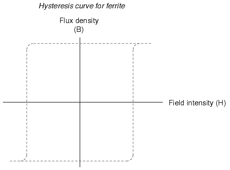
Shown on a graph with the strength of the applied magnetic field on the horizontal axis (field intensity), and the actual magnetization (orientation of electron spins in the ferrite material) on the vertical axis (flux density), ferrite won't become magnetized one direction until the applied field exceeds a critical threshold value. Once that critical value is exceeded, the electrons in the ferrite "snap" into magnetic alignment and the ferrite becomes magnetized. If the applied field is then turned off, the ferrite maintains full magnetism. To magnetize the ferrite in the other direction (polarity), the applied magnetic field must exceed the critical value in the opposite direction. Once that critical value is exceeded, the electrons in the ferrite "snap" into magnetic alignment in the opposite direction. Once again, if the applied field is then turned off, the ferrite maintains full magnetism. To put it simply, the magnetization of a piece of ferrite is "bistable."

Exploiting this strange property of ferrite, we can use this natural magnetic "latch" to store a binary bit of data. To set or reset this "latch," we can use electric current through a wire or coil to generate the necessary magnetic field, which will then be applied to the ferrite. Jay Forrester of MIT applied this principle in inventing the magnetic "core" memory, which became the dominant computer memory technology during the 1970's.

A grid of wires, electrically insulated from one another, crossed through the center of many ferrite rings, each of which being called a "core." As DC current moved through any wire from the power supply to ground, a circular magnetic field was generated around that energized wire. The resistor values were set so that the amount of current at the regulated power supply voltage would produce slightly more than 1/2 the critical magnetic field strength needed to magnetize any one of the ferrite rings. Therefore, if column #4 wire was energized, all the cores on that column would be subjected to the magnetic field from that one wire, but it would not be strong enough to change the magnetization of any of those cores. However, if column #4 wire and row #5 wire were both energized, the core at that intersection of column #4 and row #5 would be subjected to a sum of those two magnetic fields: a magnitude strong enough to "set" or "reset" the magnetization of that core. In other words, each core was addressed by the intersection of row and column. The distinction between "set" and "reset" was the direction of the core's magnetic polarity, and that bit value of data would be determined by the polarity of the voltages (with respect to ground) that the row and column wires would be energized with.

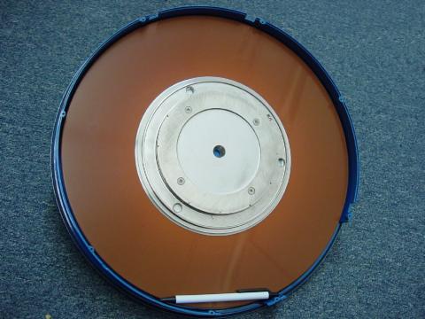
The following photograph shows a core memory board from a Data General brand, "Nova" model computer, circa late 1960's or early 1970's. It had a total storage capacity of 4 kbytes (that's kilobytes, not megabytes!). A ball-point pen is shown for size comparison:

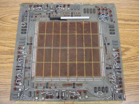
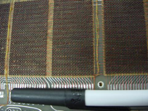
The electronic components seen around the periphery of this board are used for "driving" the column and row wires with current, and also to read the status of a core. A close-up photograph reveals the ring-shaped cores, through which the matrix wires thread. Again, a ball-point pen is shown for size comparison:

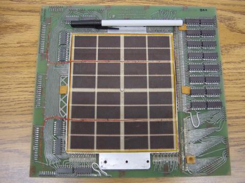
A core memory board of later design (circa 1971) is shown in the next photograph. Its cores are much smaller and more densely packed, giving more memory storage capacity than the former board (8 kbytes instead of 4 kbytes):

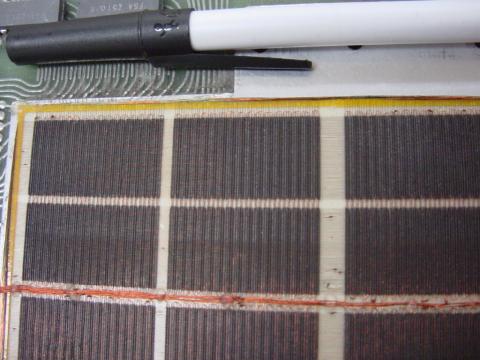
And, another close-up of the cores:

Writing data to core memory was easy enough, but reading that data was a bit of a trick. To facilitate this essential function, a "read" wire was threaded through all the cores in a memory matrix, one end of it being grounded and the other end connected to an amplifier circuit. A pulse of voltage would be generated on this "read" wire if the addressed core changed states (from 0 to 1, or 1 to 0). In other words, to read a core's value, you had to write either a 1 or a 0 to that core and monitor the voltage induced on the read wire to see if the core changed. Obviously, if the core's state was changed, you would have to re-set it back to its original state, or else the data would have been lost. This process is known as a destructive read, because data may be changed (destroyed) as it is read. Thus, refreshing is necessary with core memory, although not in every case (that is, in the case of the core's state not changing when either a 1 or a 0 was written to it).

One major advantage of core memory over delay lines and Williams Tubes was nonvolatility. The ferrite cores maintained their magnetization indefinitely, with no power or refreshing required. It was also relatively easy to build, denser, and physically more rugged than any of its predecessors. Core memory was used from the 1960's until the late 1970's in many computer systems, including the computers used for the Apollo space program, CNC machine tool control computers, business ("mainframe") computers, and industrial control systems. Despite the fact that core memory is long obsolete, the term "core" is still used sometimes with reference to a computer's RAM memory.

All the while that delay lines, Williams Tube, and core memory technologies were being invented, the simple static RAM was being improved with smaller active component (vacuum tube or transistor) technology. Static RAM was never totally eclipsed by its competitors: even the old ENIAC computer of the 1950's used vacuum tube ring-counter circuitry for data registers and computation. Eventually though, smaller and smaller scale IC chip manufacturing technology gave transistors the practical edge over other technologies, and core memory became a museum piece in the 1980's.

One last attempt at a magnetic memory better than core was the bubble memory. Bubble memory took advantage of a peculiar phenomenon in a mineral called garnet, which, when arranged in a thin film and exposed to a constant magnetic field perpendicular to the film, supported tiny regions of oppositely-magnetized "bubbles" that could be nudged along the film by prodding with other external magnetic fields. "Tracks" could be laid on the garnet to focus the movement of the bubbles by depositing magnetic material on the surface of the film. A continuous track was formed on the garnet which gave the bubbles a long loop in which to travel, and motive force was applied to the bubbles with a pair of wire coils wrapped around the garnet and energized with a 2-phase voltage. Bubbles could be created or destroyed with a tiny coil of wire strategically placed in the bubbles' path.

The presence of a bubble represented a binary "1" and the absence of a bubble represented a binary "0." Data could be read and written in this chain of moving magnetic bubbles as they passed by the tiny coil of wire, much the same as the read/write "head" in a cassette tape player, reading the magnetization of the tape as it moves. Like core memory, bubble memory was nonvolatile: a permanent magnet supplied the necessary background field needed to support the bubbles when the power was turned off. Unlike core memory, however, bubble memory had phenomenal storage density: millions of bits could be stored on a chip of garnet only a couple of square inches in size. What killed bubble memory as a viable alternative to static and dynamic RAM was its slow, sequential data access. Being nothing more than an incredibly long serial shift register (ring counter), access to any particular portion of data in the serial string could be quite slow compared to other memory technologies.

An electrostatic equivalent of the bubble memory is the Charge-Coupled Device (CCD) memory, an adaptation of the CCD devices used in digital photography. Like bubble memory, the bits are serially shifted along channels on the substrate material by clock pulses. Unlike bubble memory, the electrostatic charges decay and must be refreshed. CCD memory is therefore volatile, with high storage density and sequential access. Interesting, isn't it? The old Williams Tube memory was adapted from CRT viewing technology, and CCD memory from video recording technology.
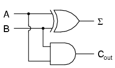
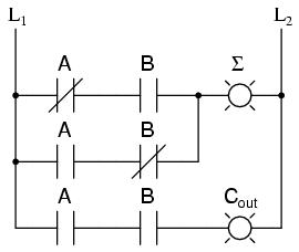
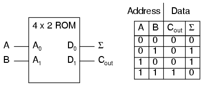
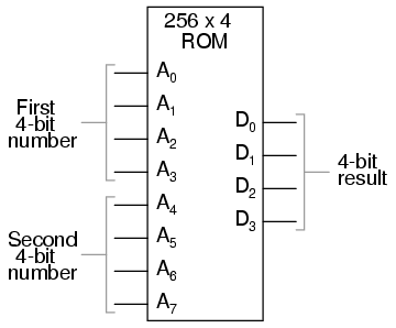
Read-only memory

Read-only memory (ROM) is similar in design to static or dynamic RAM circuits, except that the "latching" mechanism is made for one-time (or limited) operation. The simplest type of ROM is that which uses tiny "fuses" which can be selectively blown or left alone to represent the two binary states. Obviously, once one of the little fuses is blown, it cannot be made whole again, so the writing of such ROM circuits is one-time only. Because it can be written (programmed) once, these circuits are sometimes referred to as PROMs (Programmable Read-Only Memory).

However, not all writing methods are as permanent as blown fuses. If a transistor latch can be made which is resettable only with significant effort, a memory device that's something of a cross between a RAM and a ROM can be built. Such a device is given a rather oxymoronic name: the EPROM (Erasable Programmable Read-Only Memory). EPROMs come in two basic varieties: Electrically-erasable (EEPROM) and Ultraviolet-erasable (UV/EPROM). Both types of EPROMs use capacitive charge MOSFET devices to latch on or off. UV/EPROMs are "cleared" by long-term exposure to ultraviolet light. They are easy to identify: they have a transparent glass window which exposes the silicon chip material to light. Once programmed, you must cover that glass window with tape to prevent ambient light from degrading the data over time. EPROMs are often programmed using higher signal voltages than what is used during "read-only" mode.

Memory with moving parts: "Drives"

The earliest forms of digital data storage involving moving parts was that of the punched paper card. Joseph Marie Jacquard invented a weaving loom in 1780 which automatically followed weaving instructions set by carefully placed holes in paper cards. This same technology was adapted to electronic computers in the 1950's, with the cards being read mechanically (metal-to-metal contact through the holes), pneumatically (air blown through the holes, the presence of a hole sensed by air nozzle backpressure), or optically (light shining through the holes).

An improvement over paper cards is the paper tape, still used in some industrial environments (notably the CNC machine tool industry), where data storage and speed demands are low and ruggedness is highly valued. Instead of wood-fiber paper, mylar material is often used, with optical reading of the tape being the most popular method.

Magnetic tape (very similar to audio or video cassette tape) was the next logical improvement in storage media. It is still widely used today, as a means to store "backup" data for archiving and emergency restoration for other, faster methods of data storage. Like paper tape, magnetic tape is sequential access, rather than random access. In early home computer systems, regular audio cassette tape was used to store data in modulated form, the binary 1's and 0's represented by different frequencies (similar to FSK data communication). Access speed was terribly slow (if you were reading ASCII text from the tape, you could almost keep up with the pace of the letters appearing on the computer's screen!), but it was cheap and fairly reliable.

Tape suffered the disadvantage of being sequential access. To address this weak point, magnetic storage "drives" with disk- or drum-shaped media were built. An electric motor provided constant-speed motion. A movable read/write coil (also known as a "head") was provided which could be positioned via servo-motors to various locations on the height of the drum or the radius of the disk, giving access that is almost random (you might still have to wait for the drum or disk to rotate to the proper position once the read/write coil has reached the right location).

The disk shape lent itself best to portable media, and thus the floppy disk was born. Floppy disks (so-called because the magnetic media is thin and flexible) were originally made in 8-inch diameter formats. Later, the 5-1/4 inch variety was introduced, which was made practical by advances in media particle density. All things being equal, a larger disk has more space upon which to write data. However, storage density can be improved by making the little grains of iron-oxide material on the disk substrate smaller. Today, the 3-1/2 inch floppy disk is the preeminent format, with a capacity of 1.44 Mbytes (2.88 Mbytes on SCSI drives). Other portable drive formats are becoming popular, with IoMega's 100 Mbyte "ZIP" and 1 Gbyte "JAZ" disks appearing as original equipment on some personal computers.

Still, floppy drives have the disadvantage of being exposed to harsh environments, being constantly removed from the drive mechanism which reads, writes, and spins the media. The first disks were enclosed units, sealed from all dust and other particulate matter, and were definitely not portable. Keeping the media in an enclosed environment allowed engineers to avoid dust altogether, as well as spurious magnetic fields. This, in turn, allowed for much closer spacing between the head and the magnetic material, resulting in a much tighter-focused magnetic field to write data to the magnetic material.

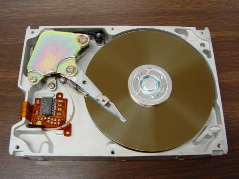
The following photograph shows a hard disk drive "platter" of approximately 30 Mbytes storage capacity. A ball-point pen has been set near the bottom of the platter for size reference:

Modern disk drives use multiple platters made of hard material (hence the name, "hard drive") with multiple read/write heads for every platter. The gap between head and platter is much smaller than the diameter of a human hair. If the hermetically-sealed environment inside a hard disk drive is contaminated with outside air, the hard drive will be rendered useless. Dust will lodge between the heads and the platters, causing damage to the surface of the media.

Here is a hard drive with four platters, although the angle of the shot only allows viewing of the top platter. This unit is complete with drive motor, read/write heads, and associated electronics. It has a storage capacity of 340 Mbytes, and is about the same length as the ball-point pen shown in the previous photograph:

While it is inevitable that non-moving-part technology will replace mechanical drives in the future, current state-of-the-art electromechanical drives continue to rival "solid-state" nonvolatile memory devices in storage density, and at a lower cost. In 1998, a 250 Mbyte hard drive was announced that was approximately the size of a quarter (smaller than the metal platter hub in the center of the last hard disk photograph)! In any case, storage density and reliability will undoubtedly continue to improve.

An incentive for digital data storage technology advancement was the advent of digitally encoded music. A joint venture between Sony and Phillips resulted in the release of the "compact audio disc" (CD) to the public in the late 1980's. This technology is a read-only type, the media being a transparent plastic disc backed by a thin film of aluminum. Binary bits are encoded as pits in the plastic which vary the path length of a low-power laser beam. Data is read by the low-power laser (the beam of which can be focused more precisely than normal light) reflecting off the aluminum to a photocell receiver.

The advantages of CDs over magnetic tape are legion. Being digital, the information is highly resistant to corruption. Being non-contact in operation, there is no wear incurred through playing. Being optical, they are immune to magnetic fields (which can easily corrupt data on magnetic tape or disks). It is possible to purchase CD "burner" drives which contain the high-power laser necessary to write to a blank disc.

Following on the heels of the music industry, the video entertainment industry has leveraged the technology of optical storage with the introduction of the Digital Video Disc, or DVD. Using a similar-sized plastic disc as the music CD, a DVD employs closer spacing of pits to achieve much greater storage density. This increased density allows feature-length movies to be encoded on DVD media, complete with trivia information about the movie, director's notes, and so on.

Much effort is being directed toward the development of a practical read/write optical disc (CD-W). Success has been found in using chemical substances whose color may be changed through exposure to bright laser light, then "read" by lower-intensity light. These optical discs are immediately identified by their characteristically colored surfaces, as opposed to the silver-colored underside of a standard CD.

READ MORE...

PRINCIPLES OF DIGITAL COMPUTING

A binary adder

Suppose we wanted to build a device that could add two binary bits together. Such a device is known as a half-adder, and its gate circuit looks like this:

The Σ symbol represents the "sum" output of the half-adder, the sum's least significant bit (LSB). Cout represents the "carry" output of the half-adder, the sum's most significant bit (MSB).

If we were to implement this same function in ladder (relay) logic, it would look like this:

Either circuit is capable of adding two binary digits together. The mathematical "rules" of how to add bits together are intrinsic to the hard-wired logic of the circuits. If we wanted to perform a different arithmetic operation with binary bits, such as multiplication, we would have to construct another circuit. The above circuit designs will only perform one function: add two binary bits together. To make them do something else would take re-wiring, and perhaps different componentry.

In this sense, digital arithmetic circuits aren't much different from analog arithmetic (operational amplifier) circuits: they do exactly what they're wired to do, no more and no less. We are not, however, restricted to designing digital computer circuits in this manner. It is possible to embed the mathematical "rules" for any arithmetic operation in the form of digital data rather than in hard-wired connections between gates. The result is unparalleled flexibility in operation, giving rise to a whole new kind of digital device: the programmable computer.

While this chapter is by no means exhaustive, it provides what I believe is a unique and interesting look at the nature of programmable computer devices, starting with two devices often overlooked in introductory textbooks: look-up table memories and finite-state machines.


Look-up tables

Having learned about digital memory devices in the last chapter, we know that it is possible to store binary data within solid-state devices. Those storage "cells" within solid-state memory devices are easily addressed by driving the "address" lines of the device with the proper binary value(s). Suppose we had a ROM memory circuit written, or programmed, with certain data, such that the address lines of the ROM served as inputs and the data lines of the ROM served as outputs, generating the characteristic response of a particular logic function. Theoretically, we could program this ROM chip to emulate whatever logic function we wanted without having to alter any wire connections or gates.

Consider the following example of a 4 x 2 bit ROM memory (a very small memory!) programmed with the functionality of a half adder:

If this ROM has been written with the above data (representing a half-adder's truth table), driving the A and B address inputs will cause the respective memory cells in the ROM chip to be enabled, thus outputting the corresponding data as the Σ (Sum) and Cout bits. Unlike the half-adder circuit built of gates or relays, this device can be set up to perform any logic function at all with two inputs and two outputs, not just the half-adder function. To change the logic function, all we would need to do is write a different table of data to another ROM chip. We could even use an EPROM chip which could be re-written at will, giving the ultimate flexibility in function.

It is vitally important to recognize the significance of this principle as applied to digital circuitry. Whereas the half-adder built from gates or relays processes the input bits to arrive at a specific output, the ROM simply remembers what the outputs should be for any given combination of inputs. This is not much different from the "times tables" memorized in grade school: rather than having to calculate the product of 5 times 6 (5 + 5 + 5 + 5 + 5 + 5 = 30), school-children are taught to remember that 5 x 6 = 30, and then expected to recall this product from memory as needed. Likewise, rather than the logic function depending on the functional arrangement of hard-wired gates or relays (hardware), it depends solely on the data written into the memory (software).

Such a simple application, with definite outputs for every input, is called a look-up table, because the memory device simply "looks up" what the output(s) should to be for any given combination of inputs states.

This application of a memory device to perform logical functions is significant for several reasons:

  • Software is much easier to change than hardware.
  • Software can be archived on various kinds of memory media (disk, tape), thus providing an easy way to document and manipulate the function in a "virtual" form; hardware can only be "archived" abstractly in the form of some kind of graphical drawing.
  • Software can be copied from one memory device (such as the EPROM chip) to another, allowing the ability for one device to "learn" its function from another device.
  • Software such as the logic function example can be designed to perform functions that would be extremely difficult to emulate with discrete logic gates (or relays!).

The usefulness of a look-up table becomes more and more evident with increasing complexity of function. Suppose we wanted to build a 4-bit adder circuit using a ROM. We'd require a ROM with 8 address lines (two 4-bit numbers to be added together), plus 4 data lines (for the signed output):

With 256 addressable memory locations in this ROM chip, we would have a fair amount of programming to do, telling it what binary output to generate for each and every combination of binary inputs. We would also run the risk of making a mistake in our programming and have it output an incorrect sum, if we weren't careful. However, the flexibility of being able to configure this function (or any function) through software alone generally outweighs that costs.

Consider some of the advanced functions we could implement with the above "adder." We know that when we add two sets of numbers in 2's complement signed notation, we risk having the answer overflow. For instance, if we try to add 0111 (decimal 7) to 0110 (decimal 6) with only a 4-bit number field, the answer we'll get is 1001 (decimal -7) instead of the correct value, 13 (7 + 6), which cannot be expressed using 4 signed bits. If we wanted to, we could avoid the strange answers given in overflow conditions by programming this look-up table circuit to output something else in conditions where we know overflow will occur (that is, in any case where the real sum would exceed +7 or -8). One alternative might be to program the ROM to output the quantity 0111 (the maximum positive value that can be represented with 4 signed bits), or any other value that we determined to be more appropriate for the application than the typical overflowed "error" value that a regular adder circuit would output. It's all up to the programmer to decide what he or she wants this circuit to do, because we are no longer limited by the constraints of logic gate functions.

The possibilities don't stop at customized logic functions, either. By adding more address lines to the 256 x 4 ROM chip, we can expand the look-up table to include multiple functions:

With two more address lines, the ROM chip will have 4 times as many addresses as before (1024 instead of 256). This ROM could be programmed so that when A8 and A9 were both low, the output data represented the sum of the two 4-bit binary numbers input on address lines A0 through A7, just as we had with the previous 256 x 4 ROM circuit. For the addresses A8=1 and A9=0, it could be programmed to output the difference (subtraction) between the first 4-bit binary number (A0 through A3) and the second binary number (A4 through A7). For the addresses A8=0 and A9=1, we could program the ROM to output the difference (subtraction) of the two numbers in reverse order (second - first rather than first - second), and finally, for the addresses A8=1 and A9=1, the ROM could be programmed to compare the two inputs and output an indication of equality or inequality. What we will have then is a device that can perform four different arithmetical operations on 4-bit binary numbers, all by "looking up" the answers programmed into it.

If we had used a ROM chip with more than two additional address lines, we could program it with a wider variety of functions to perform on the two 4-bit inputs. There are a number of operations peculiar to binary data (such as parity check or Exclusive-ORing of bits) that we might find useful to have programmed in such a look-up table.

Devices such as this, which can perform a variety of arithmetical tasks as dictated by a binary input code, are known as Arithmetic Logic Units (ALUs), and they comprise one of the essential components of computer technology. Although modern ALUs are more often constructed from very complex combinational logic (gate) circuits for reasons of speed, it should be comforting to know that the exact same functionality may be duplicated with a "dumb" ROM chip programmed with the appropriate look-up table(s). In fact, this exact approach was used by IBM engineers in 1959 with the development of the IBM 1401 and 1620 computers, which used look-up tables to perform addition, rather than binary adder circuitry. The machine was fondly known as the "CADET," which stood for "Can't Add, Doesn't Even Try."

A very common application for look-up table ROMs is in control systems where a custom mathematical function needs to be represented. Such an application is found in computer-controlled fuel injection systems for automobile engines, where the proper air/fuel mixture ratio for efficient and clean operation changes with several environmental and operational variables. Tests performed on engines in research laboratories determine what these ideal ratios are for varying conditions of engine load, ambient air temperature, and barometric air pressure. The variables are measured with sensor transducers, their analog outputs converted to digital signals with A/D circuitry, and those parallel digital signals used as address inputs to a high-capacity ROM chip programmed to output the optimum digital value for air/fuel ratio for any of these given conditions.

Sometimes, ROMs are used to provide one-dimensional look-up table functions, for "correcting" digitized signal values so that they more accurately represent their real-world significance. An example of such a device is a thermocouple transmitter, which measures the millivoltage signal generated by a junction of dissimilar metals and outputs a signal which is supposed to directly correspond to that junction temperature. Unfortunately, thermocouple junctions do not have perfectly linear temperature/voltage responses, and so the raw voltage signal is not perfectly proportional to temperature. By digitizing the voltage signal (A/D conversion) and sending that digital value to the address of a ROM programmed with the necessary correction values, the ROM's programming could eliminate some of the nonlinearity of the thermocouple's temperature-to-millivoltage relationship, so that the final output of the device would be more accurate. The popular instrumentation term for such a look-up table is a digital characterizer.

Another application for look-up tables is in special code translation. A 128 x 8 ROM, for instance, could be used to translate 7-bit ASCII code to 8-bit EBCDIC code:

Again, all that is required is for the ROM chip to be properly programmed with the necessary data so that each valid ASCII input will produce a corresponding EBCDIC output code.

Finite-state machines

Feedback is a fascinating engineering principle. It can turn a rather simple device or process into something substantially more complex. We've seen the effects of feedback intentionally integrated into circuit designs with some rather astounding effects:

  • Comparator + negative feedback -----------> controllable-gain amplifier
  • Comparator + positive feedback -----------> comparator with hysteresis
  • Combinational logic + positive feedback --> multivibrator

In the field of process instrumentation, feedback is used to transform a simple measurement system into something capable of control:

  • Measurement system + negative feedback ---> closed-loop control system

Feedback, both positive and negative, has the tendency to add whole new dynamics to the operation of a device or system. Sometimes, these new dynamics find useful application, while other times they are merely interesting. With look-up tables programmed into memory devices, feedback from the data outputs back to the address inputs creates a whole new type of device: the Finite State Machine, or FSM:

The above circuit illustrates the basic idea: the data stored at each address becomes the next storage location that the ROM gets addressed to. The result is a specific sequence of binary numbers (following the sequence programmed into the ROM) at the output, over time. To avoid signal timing problems, though, we need to connect the data outputs back to the address inputs through a 4-bit D-type flip-flop, so that the sequence takes place step by step to the beat of a controlled clock pulse:

An analogy for the workings of such a device might be an array of post-office boxes, each one with an identifying number on the door (the address), and each one containing a piece of paper with the address of another P.O. box written on it (the data). A person, opening the first P.O. box, would find in it the address of the next P.O. box to open. By storing a particular pattern of addresses in the P.O. boxes, we can dictate the sequence in which each box gets opened, and therefore the sequence of which paper gets read.

Having 16 addressable memory locations in the ROM, this Finite State Machine would have 16 different stable "states" in which it could latch. In each of those states, the identity of the next state would be programmed in to the ROM, awaiting the signal of the next clock pulse to be fed back to the ROM as an address. One useful application of such an FSM would be to generate an arbitrary count sequence, such as Gray Code:


Address  -----> Data          Gray Code count sequence:
0000 -------> 0001 0 0000
0001 -------> 0011 1 0001
0010 -------> 0110 2 0011
0011 -------> 0010 3 0010
0100 -------> 1100 4 0110
0101 -------> 0100 5 0111
0110 -------> 0111 6 0101
0111 -------> 0101 7 0100
1000 -------> 0000 8 1100
1001 -------> 1000 9 1101
1010 -------> 1011 10 1111
1011 -------> 1001 11 1110
1100 -------> 1101 12 1010
1101 -------> 1111 13 1011
1110 -------> 1010 14 1001
1111 -------> 1110 15 1000


Try to follow the Gray Code count sequence as the FSM would do it: starting at 0000, follow the data stored at that address (0001) to the next address, and so on (0011), and so on (0010), and so on (0110), etc. The result, for the program table shown, is that the sequence of addressing jumps around from address to address in what looks like a haphazard fashion, but when you check each address that is accessed, you will find that it follows the correct order for 4-bit Gray code. When the FSM arrives at its last programmed state (address 1000), the data stored there is 0000, which starts the whole sequence over again at address 0000 in step with the next clock pulse.

We could expand on the capabilities of the above circuit by using a ROM with more address lines, and adding more programming data:

Now, just like the look-up table adder circuit that we turned into an Arithmetic Logic Unit (+, -, x, / functions) by utilizing more address lines as "function control" inputs, this FSM counter can be used to generate more than one count sequence, a different sequence programmed for the four feedback bits (A0 through A3) for each of the two function control line input combinations (A4 = 0 or 1).


Address  -----> Data            Address  -----> Data
00000 -------> 0001 10000 -------> 0001
00001 -------> 0010 10001 -------> 0011
00010 -------> 0011 10010 -------> 0110
00011 -------> 0100 10011 -------> 0010
00100 -------> 0101 10100 -------> 1100
00101 -------> 0110 10101 -------> 0100
00110 -------> 0111 10110 -------> 0111
00111 -------> 1000 10111 -------> 0101
01000 -------> 1001 11000 -------> 0000
01001 -------> 1010 11001 -------> 1000
01010 -------> 1011 11010 -------> 1011
01011 -------> 1100 11011 -------> 1001
01100 -------> 1101 11100 -------> 1101
01101 -------> 1110 11101 -------> 1111
01110 -------> 1111 11110 -------> 1010
01111 -------> 0000 11111 -------> 1110


If A4 is 0, the FSM counts in binary; if A4 is 1, the FSM counts in Gray Code. In either case, the counting sequence is arbitrary: determined by the whim of the programmer. For that matter, the counting sequence doesn't even have to have 16 steps, as the programmer may decide to have the sequence recycle to 0000 at any one of the steps at all. It is a completely flexible counting device, the behavior strictly determined by the software (programming) in the ROM.

We can expand on the capabilities of the FSM even more by utilizing a ROM chip with additional address input and data output lines. Take the following circuit, for example:

Here, the D0 through D3 data outputs are used exclusively for feedback to the A0 through A3 address lines. Date output lines D4 through D7 can be programmed to output something other than the FSM's "state" value. Being that four data output bits are being fed back to four address bits, this is still a 16-state device. However, having the output data come from other data output lines gives the programmer more freedom to configure functions than before. In other words, this device can do far more than just count! The programmed output of this FSM is dependent not only upon the state of the feedback address lines (A0 through A3), but also the states of the input lines (A4 through A7). The D-type flip/flop's clock signal input does not have to come from a pulse generator, either. To make things more interesting, the flip/flop could be wired up to clock on some external event, so that the FSM goes to the next state only when an input signal tells it to.

Now we have a device that better fulfills the meaning of the word "programmable." The data written to the ROM is a program in the truest sense: the outputs follow a pre-established order based on the inputs to the device and which "step" the device is on in its sequence. This is very close to the operating design of the Turing Machine, a theoretical computing device invented by Alan Turing, mathematically proven to be able to solve any known arithmetic problem, given enough memory capacity.

Microprocessors

Early computer science pioneers such as Alan Turing and John Von Neumann postulated that for a computing device to be really useful, it not only had to be able to generate specific outputs as dictated by programmed instructions, but it also had to be able to write data to memory, and be able to act on that data later. Both the program steps and the processed data were to reside in a common memory "pool," thus giving way to the label of the stored-program computer. Turing's theoretical machine utilized a sequential-access tape, which would store data for a control circuit to read, the control circuit re-writing data to the tape and/or moving the tape to a new position to read more data. Modern computers use random-access memory devices instead of sequential-access tapes to accomplish essentially the same thing, except with greater capability.

A helpful illustration is that of early automatic machine tool control technology. Called open-loop, or sometimes just NC (numerical control), these control systems would direct the motion of a machine tool such as a lathe or a mill by following instructions programmed as holes in paper tape. The tape would be run one direction through a "read" mechanism, and the machine would blindly follow the instructions on the tape without regard to any other conditions. While these devices eliminated the burden of having to have a human machinist direct every motion of the machine tool, it was limited in usefulness. Because the machine was blind to the real world, only following the instructions written on the tape, it could not compensate for changing conditions such as expansion of the metal or wear of the mechanisms. Also, the tape programmer had to be acutely aware of the sequence of previous instructions in the machine's program to avoid troublesome circumstances (such as telling the machine tool to move the drill bit laterally while it is still inserted into a hole in the work), since the device had no memory other than the tape itself, which was read-only. Upgrading from a simple tape reader to a Finite State control design gave the device a sort of memory that could be used to keep track of what it had already done (through feedback of some of the data bits to the address bits), so at least the programmer could decide to have the circuit remember "states" that the machine tool could be in (such as "coolant on," or tool position). However, there was still room for improvement.

The ultimate approach is to have the program give instructions which would include the writing of new data to a read/write (RAM) memory, which the program could easily recall and process. This way, the control system could record what it had done, and any sensor-detectable process changes, much in the same way that a human machinist might jot down notes or measurements on a scratch-pad for future reference in his or her work. This is what is referred to as CNC, or Closed-loop Numerical Control.

Engineers and computer scientists looked forward to the possibility of building digital devices that could modify their own programming, much the same as the human brain adapts the strength of inter-neural connections depending on environmental experiences (that is why memory retention improves with repeated study, and behavior is modified through consequential feedback). Only if the computer's program were stored in the same writable memory "pool" as the data would this be practical. It is interesting to note that the notion of a self-modifying program is still considered to be on the cutting edge of computer science. Most computer programming relies on rather fixed sequences of instructions, with a separate field of data being the only information that gets altered.

To facilitate the stored-program approach, we require a device that is much more complex than the simple FSM, although many of the same principles apply. First, we need read/write memory that can be easily accessed: this is easy enough to do. Static or dynamic RAM chips do the job well, and are inexpensive. Secondly, we need some form of logic to process the data stored in memory. Because standard and Boolean arithmetic functions are so useful, we can use an Arithmetic Logic Unit (ALU) such as the look-up table ROM example explored earlier. Finally, we need a device that controls how and where data flows between the memory, the ALU, and the outside world. This so-called Control Unit is the most mysterious piece of the puzzle yet, being comprised of tri-state buffers (to direct data to and from buses) and decoding logic which interprets certain binary codes as instructions to carry out. Sample instructions might be something like: "add the number stored at memory address 0010 with the number stored at memory address 1101," or, "determine the parity of the data in memory address 0111." The choice of which binary codes represent which instructions for the Control Unit to decode is largely arbitrary, just as the choice of which binary codes to use in representing the letters of the alphabet in the ASCII standard was largely arbitrary. ASCII, however, is now an internationally recognized standard, whereas control unit instruction codes are almost always manufacturer-specific.

Putting these components together (read/write memory, ALU, and control unit) results in a digital device that is typically called a processor. If minimal memory is used, and all the necessary components are contained on a single integrated circuit, it is called a microprocessor. When combined with the necessary bus-control support circuitry, it is known as a Central Processing Unit, or CPU.

CPU operation is summed up in the so-called fetch/execute cycle. Fetch means to read an instruction from memory for the Control Unit to decode. A small binary counter in the CPU (known as the program counter or instruction pointer) holds the address value where the next instruction is stored in main memory. The Control Unit sends this binary address value to the main memory's address lines, and the memory's data output is read by the Control Unit to send to another holding register. If the fetched instruction requires reading more data from memory (for example, in adding two numbers together, we have to read both the numbers that are to be added from main memory or from some other source), the Control Unit appropriately addresses the location of the requested data and directs the data output to ALU registers. Next, the Control Unit would execute the instruction by signaling the ALU to do whatever was requested with the two numbers, and direct the result to another register called the accumulator. The instruction has now been "fetched" and "executed," so the Control Unit now increments the program counter to step the next instruction, and the cycle repeats itself.


        Microprocessor (CPU)

--------------------------------------
| ** Program counter ** |
| (increments address value sent to |
| external memory chip(s) to fetch |==========> Address bus
| the next instruction) | (to RAM memory)
--------------------------------------
| ** Control Unit ** |<=========> Control Bus
| (decodes instructions read from | (to all devices sharing
| program in memory, enables flow | address and/or data busses;
| of data to and from ALU, internal | arbitrates all bus communi-
| registers, and external devices) | cations)
--------------------------------------
| ** Arithmetic Logic Unit (ALU) ** |
| (performs all mathematical |
| calculations and Boolean |
| functions) |
--------------------------------------
| ** Registers ** |
| (small read/write memories for |<=========> Data Bus
| holding instruction codes, | (from RAM memory and other
| error codes, ALU data, etc; | external devices)
| includes the "accumulator") |
--------------------------------------


As one might guess, carrying out even simple instructions is a tedious process. Several steps are necessary for the Control Unit to complete the simplest of mathematical procedures. This is especially true for arithmetic procedures such as exponents, which involve repeated executions ("iterations") of simpler functions. Just imagine the sheer quantity of steps necessary within the CPU to update the bits of information for the graphic display on a flight simulator game! The only thing which makes such a tedious process practical is the fact that microprocessor circuits are able to repeat the fetch/execute cycle with great speed.

In some microprocessor designs, there are minimal programs stored within a special ROM memory internal to the device (called microcode) which handle all the sub-steps necessary to carry out more complex math operations. This way, only a single instruction has to be read from the program RAM to do the task, and the programmer doesn't have to deal with trying to tell the microprocessor how to do every minute step. In essence, its a processor inside of a processor; a program running inside of a program.

Microprocessor programming

The "vocabulary" of instructions which any particular microprocessor chip possesses is specific to that model of chip. An Intel 80386, for example, uses a completely different set of binary codes than a Motorola 68020, for designating equivalent functions. Unfortunately, there are no standards in place for microprocessor instructions. This makes programming at the very lowest level very confusing and specialized.

When a human programmer develops a set of instructions to directly tell a microprocessor how to do something (like automatically control the fuel injection rate to an engine), they're programming in the CPU's own "language." This language, which consists of the very same binary codes which the Control Unit inside the CPU chip decodes to perform tasks, is often referred to as machine language. While machine language software can be "worded" in binary notation, it is often written in hexadecimal form, because it is easier for human beings to work with. For example, I'll present just a few of the common instruction codes for the Intel 8080 micro-processor chip:


Hexadecimal    Binary              Instruction description
----------- -------- -----------------------------------------
| 7B 01111011 Move contents of register A to register E
|
| 87 10000111 Add contents of register A to register D
|
| 1C 00011100 Increment the contents of register E by 1
|
| D3 11010011 Output byte of data to data bus


Even with hexadecimal notation, these instructions can be easily confused and forgotten. For this purpose, another aid for programmers exists called assembly language. With assembly language, two to four letter mnemonic words are used in place of the actual hex or binary code for describing program steps. For example, the instruction 7B for the Intel 8080 would be "MOV A,E" in assembly language. The mnemonics, of course, are useless to the microprocessor, which can only understand binary codes, but it is an expedient way for programmers to manage the writing of their programs on paper or text editor (word processor). There are even programs written for computers called assemblers which understand these mnemonics, translating them to the appropriate binary codes for a specified target microprocessor, so that the programmer can write a program in the computer's native language without ever having to deal with strange hex or tedious binary code notation.

Once a program is developed by a person, it must be written into memory before a microprocessor can execute it. If the program is to be stored in ROM (which some are), this can be done with a special machine called a ROM programmer, or (if you're masochistic), by plugging the ROM chip into a breadboard, powering it up with the appropriate voltages, and writing data by making the right wire connections to the address and data lines, one at a time, for each instruction. If the program is to be stored in volatile memory, such as the operating computer's RAM memory, there may be a way to type it in by hand through that computer's keyboard (some computers have a mini-program stored in ROM which tells the microprocessor how to accept keystrokes from a keyboard and store them as commands in RAM), even if it is too dumb to do anything else. Many "hobby" computer kits work like this. If the computer to be programmed is a fully-functional personal computer with an operating system, disk drives, and the whole works, you can simply command the assembler to store your finished program onto a disk for later retrieval. To "run" your program, you would simply type your program's filename at the prompt, press the Enter key, and the microprocessor's Program Counter register would be set to point to the location ("address") on the disk where the first instruction is stored, and your program would run from there.

Although programming in machine language or assembly language makes for fast and highly efficient programs, it takes a lot of time and skill to do so for anything but the simplest tasks, because each machine language instruction is so crude. The answer to this is to develop ways for programmers to write in "high level" languages, which can more efficiently express human thought. Instead of typing in dozens of cryptic assembly language codes, a programmer writing in a high-level language would be able to write something like this . . .


Print "Hello, world!"


. . . and expect the computer to print "Hello, world!" with no further instruction on how to do so. This is a great idea, but how does a microprocessor understand such "human" thinking when its vocabulary is so limited?

The answer comes in two different forms: interpretation, or compilation. Just like two people speaking different languages, there has to be some way to transcend the language barrier in order for them to converse. A translator is needed to translate each person's words to the other person's language, one way at a time. For the microprocessor, this means another program, written by another programmer in machine language, which recognizes the ASCII character patterns of high-level commands such as Print (P-r-i-n-t) and can translate them into the necessary bite-size steps that the microprocessor can directly understand. If this translation is done during program execution, just like a translator intervening between two people in a live conversation, it is called "interpretation." On the other hand, if the entire program is translated to machine language in one fell swoop, like a translator recording a monologue on paper and then translating all the words at one sitting into a written document in the other language, the process is called "compilation."

Interpretation is simple, but makes for a slow-running program because the microprocessor has to continually translate the program between steps, and that takes time. Compilation takes time initially to translate the whole program into machine code, but the resulting machine code needs no translation after that and runs faster as a consequence. Programming languages such as BASIC and FORTH are interpreted. Languages such as C, C++, FORTRAN, and PASCAL are compiled. Compiled languages are generally considered to be the languages of choice for professional programmers, because of the efficiency of the final product.

Naturally, because machine language vocabularies vary widely from microprocessor to microprocessor, and since high-level languages are designed to be as universal as possible, the interpreting and compiling programs necessary for language translation must be microprocessor-specific. Development of these interpreters and compilers is a most impressive feat: the people who make these programs most definitely earn their keep, especially when you consider the work they must do to keep their software product current with the rapidly-changing microprocessor models appearing on the market!

To mitigate this difficulty, the trend-setting manufacturers of microprocessor chips (most notably, Intel and Motorola) try to design their new products to be backwardly compatible with their older products. For example, the entire instruction set for the Intel 80386 chip is contained within the latest Pentium IV chips, although the Pentium chips have additional instructions that the 80386 chips lack. What this means is that machine-language programs (compilers, too) written for 80386 computers will run on the latest and greatest Intel Pentium IV CPU, but machine-language programs written specifically to take advantage of the Pentium's larger instruction set will not run on an 80386, because the older CPU simply doesn't have some of those instructions in its vocabulary: the Control Unit inside the 80386 cannot decode them.

Building on this theme, most compilers have settings that allow the programmer to select which CPU type he or she wants to compile machine-language code for. If they select the 80386 setting, the compiler will perform the translation using only instructions known to the 80386 chip; if they select the Pentium setting, the compiler is free to make use of all instructions known to Pentiums. This is analogous to telling a translator what minimum reading level their audience will be: a document translated for a child will be understandable to an adult, but a document translated for an adult may very well be gibberish to a child.

READ MORE...

DIGITAL-ANALOG CONVERSION

Introduction

Connecting digital circuitry to sensor devices is simple if the sensor devices are inherently digital themselves. Switches, relays, and encoders are easily interfaced with gate circuits due to the on/off nature of their signals. However, when analog devices are involved, interfacing becomes much more complex. What is needed is a way to electronically translate analog signals into digital (binary) quantities, and vice versa. An analog-to-digital converter, or ADC, performs the former task while a digital-to-analog converter, or DAC, performs the latter.

An ADC inputs an analog electrical signal such as voltage or current and outputs a binary number. In block diagram form, it can be represented as such:

A DAC, on the other hand, inputs a binary number and outputs an analog voltage or current signal. In block diagram form, it looks like this:

Together, they are often used in digital systems to provide complete interface with analog sensors and output devices for control systems such as those used in automotive engine controls:

It is much easier to convert a digital signal into an analog signal than it is to do the reverse. Therefore, we will begin with DAC circuitry and then move to ADC circuitry.

The R/2nR DAC

This DAC circuit, otherwise known as the binary-weighted-input DAC, is a variation on the inverting summer op-amp circuit. If you recall, the classic inverting summer circuit is an operational amplifier using negative feedback for controlled gain, with several voltage inputs and one voltage output. The output voltage is the inverted (opposite polarity) sum of all input voltages:

For a simple inverting summer circuit, all resistors must be of equal value. If any of the input resistors were different, the input voltages would have different degrees of effect on the output, and the output voltage would not be a true sum. Let's consider, however, intentionally setting the input resistors at different values. Suppose we were to set the input resistor values at multiple powers of two: R, 2R, and 4R, instead of all the same value R:

Starting from V1 and going through V3, this would give each input voltage exactly half the effect on the output as the voltage before it. In other words, input voltage V1 has a 1:1 effect on the output voltage (gain of 1), while input voltage V2 has half that much effect on the output (a gain of 1/2), and V3 half of that (a gain of 1/4). These ratios are were not arbitrarily chosen: they are the same ratios corresponding to place weights in the binary numeration system. If we drive the inputs of this circuit with digital gates so that each input is either 0 volts or full supply voltage, the output voltage will be an analog representation of the binary value of these three bits.

If we chart the output voltages for all eight combinations of binary bits (000 through 111) input to this circuit, we will get the following progression of voltages:


---------------------------------
| Binary | Output voltage |
---------------------------------
| 000 | 0.00 V |
---------------------------------
| 001 | -1.25 V |
---------------------------------
| 010 | -2.50 V |
---------------------------------
| 011 | -3.75 V |
---------------------------------
| 100 | -5.00 V |
---------------------------------
| 101 | -6.25 V |
---------------------------------
| 110 | -7.50 V |
---------------------------------
| 111 | -8.75 V |
---------------------------------


Note that with each step in the binary count sequence, there results a 1.25 volt change in the output. This circuit is very easy to simulate using SPICE. In the following simulation, I set up the DAC circuit with a binary input of 110 (note the first node numbers for resistors R1, R2, and R3: a node number of "1" connects it to the positive side of a 5 volt battery, and a node number of "0" connects it to ground). The output voltage appears on node 6 in the simulation:


binary-weighted dac   
v1 1 0 dc 5
rbogus 1 0 99k
r1 1 5 1k
r2 1 5 2k
r3 0 5 4k
rfeedbk 5 6 1k
e1 6 0 5 0 999k
.end

node voltage node voltage node voltage
(1) 5.0000 (5) 0.0000 (6) -7.5000


We can adjust resistors values in this circuit to obtain output voltages directly corresponding to the binary input. For example, by making the feedback resistor 800 Ω instead of 1 kΩ, the DAC will output -1 volt for the binary input 001, -4 volts for the binary input 100, -7 volts for the binary input 111, and so on.


(with feedback resistor set at 800 ohms)
---------------------------------
| Binary | Output voltage |
---------------------------------
| 000 | 0.00 V |
---------------------------------
| 001 | -1.00 V |
---------------------------------
| 010 | -2.00 V |
---------------------------------
| 011 | -3.00 V |
---------------------------------
| 100 | -4.00 V |
---------------------------------
| 101 | -5.00 V |
---------------------------------
| 110 | -6.00 V |
---------------------------------
| 111 | -7.00 V |
---------------------------------


If we wish to expand the resolution of this DAC (add more bits to the input), all we need to do is add more input resistors, holding to the same power-of-two sequence of values:

It should be noted that all logic gates must output exactly the same voltages when in the "high" state. If one gate is outputting +5.02 volts for a "high" while another is outputting only +4.86 volts, the analog output of the DAC will be adversely affected. Likewise, all "low" voltage levels should be identical between gates, ideally 0.00 volts exactly. It is recommended that CMOS output gates are used, and that input/feedback resistor values are chosen so as to minimize the amount of current each gate has to source or sink.

The R/2R DAC

An alternative to the binary-weighted-input DAC is the so-called R/2R DAC, which uses fewer unique resistor values. A disadvantage of the former DAC design was its requirement of several different precise input resistor values: one unique value per binary input bit. Manufacture may be simplified if there are fewer different resistor values to purchase, stock, and sort prior to assembly.

Of course, we could take our last DAC circuit and modify it to use a single input resistance value, by connecting multiple resistors together in series:

Unfortunately, this approach merely substitutes one type of complexity for another: volume of components over diversity of component values. There is, however, a more efficient design methodology.

By constructing a different kind of resistor network on the input of our summing circuit, we can achieve the same kind of binary weighting with only two kinds of resistor values, and with only a modest increase in resistor count. This "ladder" network looks like this:

Mathematically analyzing this ladder network is a bit more complex than for the previous circuit, where each input resistor provided an easily-calculated gain for that bit. For those who are interested in pursuing the intricacies of this circuit further, you may opt to use Thevenin's theorem for each binary input (remember to consider the effects of the virtual ground), and/or use a simulation program like SPICE to determine circuit response. Either way, you should obtain the following table of figures:


---------------------------------
| Binary | Output voltage |
---------------------------------
| 000 | 0.00 V |
---------------------------------
| 001 | -1.25 V |
---------------------------------
| 010 | -2.50 V |
---------------------------------
| 011 | -3.75 V |
---------------------------------
| 100 | -5.00 V |
---------------------------------
| 101 | -6.25 V |
---------------------------------
| 110 | -7.50 V |
---------------------------------
| 111 | -8.75 V |
---------------------------------


As was the case with the binary-weighted DAC design, we can modify the value of the feedback resistor to obtain any "span" desired. For example, if we're using +5 volts for a "high" voltage level and 0 volts for a "low" voltage level, we can obtain an analog output directly corresponding to the binary input (011 = -3 volts, 101 = -5 volts, 111 = -7 volts, etc.) by using a feedback resistance with a value of 1.6R instead of 2R.

Flash ADC

Also called the parallel A/D converter, this circuit is the simplest to understand. It is formed of a series of comparators, each one comparing the input signal to a unique reference voltage. The comparator outputs connect to the inputs of a priority encoder circuit, which then produces a binary output. The following illustration shows a 3-bit flash ADC circuit:

Vref is a stable reference voltage provided by a precision voltage regulator as part of the converter circuit, not shown in the schematic. As the analog input voltage exceeds the reference voltage at each comparator, the comparator outputs will sequentially saturate to a high state. The priority encoder generates a binary number based on the highest-order active input, ignoring all other active inputs.

When operated, the flash ADC produces an output that looks something like this:

For this particular application, a regular priority encoder with all its inherent complexity isn't necessary. Due to the nature of the sequential comparator output states (each comparator saturating "high" in sequence from lowest to highest), the same "highest-order-input selection" effect may be realized through a set of Exclusive-OR gates, allowing the use of a simpler, non-priority encoder:

And, of course, the encoder circuit itself can be made from a matrix of diodes, demonstrating just how simply this converter design may be constructed:

Not only is the flash converter the simplest in terms of operational theory, but it is the most efficient of the ADC technologies in terms of speed, being limited only in comparator and gate propagation delays. Unfortunately, it is the most component-intensive for any given number of output bits. This three-bit flash ADC requires eight comparators. A four-bit version would require 16 comparators. With each additional output bit, the number of required comparators doubles. Considering that eight bits is generally considered the minimum necessary for any practical ADC (256 comparators needed!), the flash methodology quickly shows its weakness.

An additional advantage of the flash converter, often overlooked, is the ability for it to produce a non-linear output. With equal-value resistors in the reference voltage divider network, each successive binary count represents the same amount of analog signal increase, providing a proportional response. For special applications, however, the resistor values in the divider network may be made non-equal. This gives the ADC a custom, nonlinear response to the analog input signal. No other ADC design is able to grant this signal-conditioning behavior with just a few component value changes.

Digital ramp ADC

Also known as the stairstep-ramp, or simply counter A/D converter, this is also fairly easy to understand but unfortunately suffers from several limitations.

The basic idea is to connect the output of a free-running binary counter to the input of a DAC, then compare the analog output of the DAC with the analog input signal to be digitized and use the comparator's output to tell the counter when to stop counting and reset. The following schematic shows the basic idea:

As the counter counts up with each clock pulse, the DAC outputs a slightly higher (more positive) voltage. This voltage is compared against the input voltage by the comparator. If the input voltage is greater than the DAC output, the comparator's output will be high and the counter will continue counting normally. Eventually, though, the DAC output will exceed the input voltage, causing the comparator's output to go low. This will cause two things to happen: first, the high-to-low transition of the comparator's output will cause the shift register to "load" whatever binary count is being output by the counter, thus updating the ADC circuit's output; secondly, the counter will receive a low signal on the active-low LOAD input, causing it to reset to 00000000 on the next clock pulse.

The effect of this circuit is to produce a DAC output that ramps up to whatever level the analog input signal is at, output the binary number corresponding to that level, and start over again. Plotted over time, it looks like this:

Note how the time between updates (new digital output values) changes depending on how high the input voltage is. For low signal levels, the updates are rather close-spaced. For higher signal levels, they are spaced further apart in time:

For many ADC applications, this variation in update frequency (sample time) would not be acceptable. This, and the fact that the circuit's need to count all the way from 0 at the beginning of each count cycle makes for relatively slow sampling of the analog signal, places the digital-ramp ADC at a disadvantage to other counter strategies.

Successive approximation ADC

One method of addressing the digital ramp ADC's shortcomings is the so-called successive-approximation ADC. The only change in this design is a very special counter circuit known as a successive-approximation register. Instead of counting up in binary sequence, this register counts by trying all values of bits starting with the most-significant bit and finishing at the least-significant bit. Throughout the count process, the register monitors the comparator's output to see if the binary count is less than or greater than the analog signal input, adjusting the bit values accordingly. The way the register counts is identical to the "trial-and-fit" method of decimal-to-binary conversion, whereby different values of bits are tried from MSB to LSB to get a binary number that equals the original decimal number. The advantage to this counting strategy is much faster results: the DAC output converges on the analog signal input in much larger steps than with the 0-to-full count sequence of a regular counter.

Without showing the inner workings of the successive-approximation register (SAR), the circuit looks like this:

It should be noted that the SAR is generally capable of outputting the binary number in serial (one bit at a time) format, thus eliminating the need for a shift register. Plotted over time, the operation of a successive-approximation ADC looks like this:

Note how the updates for this ADC occur at regular intervals, unlike the digital ramp ADC circuit.

Tracking ADC

A third variation on the counter-DAC-based converter theme is, in my estimation, the most elegant. Instead of a regular "up" counter driving the DAC, this circuit uses an up/down counter. The counter is continuously clocked, and the up/down control line is driven by the output of the comparator. So, when the analog input signal exceeds the DAC output, the counter goes into the "count up" mode. When the DAC output exceeds the analog input, the counter switches into the "count down" mode. Either way, the DAC output always counts in the proper direction to track the input signal.

Notice how no shift register is needed to buffer the binary count at the end of a cycle. Since the counter's output continuously tracks the input (rather than counting to meet the input and then resetting back to zero), the binary output is legitimately updated with every clock pulse.

An advantage of this converter circuit is speed, since the counter never has to reset. Note the behavior of this circuit:

Note the much faster update time than any of the other "counting" ADC circuits. Also note how at the very beginning of the plot where the counter had to "catch up" with the analog signal, the rate of change for the output was identical to that of the first counting ADC. Also, with no shift register in this circuit, the binary output would actually ramp up rather than jump from zero to an accurate count as it did with the counter and successive approximation ADC circuits.

Perhaps the greatest drawback to this ADC design is the fact that the binary output is never stable: it always switches between counts with every clock pulse, even with a perfectly stable analog input signal. This phenomenon is informally known as bit bobble, and it can be problematic in some digital systems.

This tendency can be overcome, though, through the creative use of a shift register. For example, the counter's output may be latched through a parallel-in/parallel-out shift register only when the output changes by two or more steps. Building a circuit to detect two or more successive counts in the same direction takes a little ingenuity, but is worth the effort.

Slope (integrating) ADC

So far, we've only been able to escape the sheer volume of components in the flash converter by using a DAC as part of our ADC circuitry. However, this is not our only option. It is possible to avoid using a DAC if we substitute an analog ramping circuit and a digital counter with precise timing.

The is the basic idea behind the so-called single-slope, or integrating ADC. Instead of using a DAC with a ramped output, we use an op-amp circuit called an integrator to generate a sawtooth waveform which is then compared against the analog input by a comparator. The time it takes for the sawtooth waveform to exceed the input signal voltage level is measured by means of a digital counter clocked with a precise-frequency square wave (usually from a crystal oscillator). The basic schematic diagram is shown here:

The IGFET capacitor-discharging transistor scheme shown here is a bit oversimplified. In reality, a latching circuit timed with the clock signal would most likely have to be connected to the IGFET gate to ensure full discharge of the capacitor when the comparator's output goes high. The basic idea, however, is evident in this diagram. When the comparator output is low (input voltage greater than integrator output), the integrator is allowed to charge the capacitor in a linear fashion. Meanwhile, the counter is counting up at a rate fixed by the precision clock frequency. The time it takes for the capacitor to charge up to the same voltage level as the input depends on the input signal level and the combination of -Vref, R, and C. When the capacitor reaches that voltage level, the comparator output goes high, loading the counter's output into the shift register for a final output. The IGFET is triggered "on" by the comparator's high output, discharging the capacitor back to zero volts. When the integrator output voltage falls to zero, the comparator output switches back to a low state, clearing the counter and enabling the integrator to ramp up voltage again.

This ADC circuit behaves very much like the digital ramp ADC, except that the comparator reference voltage is a smooth sawtooth waveform rather than a "stairstep:"

The single-slope ADC suffers all the disadvantages of the digital ramp ADC, with the added drawback of calibration drift. The accurate correspondence of this ADC's output with its input is dependent on the voltage slope of the integrator being matched to the counting rate of the counter (the clock frequency). With the digital ramp ADC, the clock frequency had no effect on conversion accuracy, only on update time. In this circuit, since the rate of integration and the rate of count are independent of each other, variation between the two is inevitable as it ages, and will result in a loss of accuracy. The only good thing to say about this circuit is that it avoids the use of a DAC, which reduces circuit complexity.

An answer to this calibration drift dilemma is found in a design variation called the dual-slope converter. In the dual-slope converter, an integrator circuit is driven positive and negative in alternating cycles to ramp down and then up, rather than being reset to 0 volts at the end of every cycle. In one direction of ramping, the integrator is driven by the positive analog input signal (producing a negative, variable rate of output voltage change, or output slope) for a fixed amount of time, as measured by a counter with a precision frequency clock. Then, in the other direction, with a fixed reference voltage (producing a fixed rate of output voltage change) with time measured by the same counter. The counter stops counting when the integrator's output reaches the same voltage as it was when it started the fixed-time portion of the cycle. The amount of time it takes for the integrator's capacitor to discharge back to its original output voltage, as measured by the magnitude accrued by the counter, becomes the digital output of the ADC circuit.

The dual-slope method can be thought of analogously in terms of a rotary spring such as that used in a mechanical clock mechanism. Imagine we were building a mechanism to measure the rotary speed of a shaft. Thus, shaft speed is our "input signal" to be measured by this device. The measurement cycle begins with the spring in a relaxed state. The spring is then turned, or "wound up," by the rotating shaft (input signal) for a fixed amount of time. This places the spring in a certain amount of tension proportional to the shaft speed: a greater shaft speed corresponds to a faster rate of winding. and a greater amount of spring tension accumulated over that period of time. After that, the spring is uncoupled from the shaft and allowed to unwind at a fixed rate, the time for it to unwind back to a relaxed state measured by a timer device. The amount of time it takes for the spring to unwind at that fixed rate will be directly proportional to the speed at which it was wound (input signal magnitude) during the fixed-time portion of the cycle.

This technique of analog-to-digital conversion escapes the calibration drift problem of the single-slope ADC because both the integrator's integration coefficient (or "gain") and the counter's rate of speed are in effect during the entire "winding" and "unwinding" cycle portions. If the counter's clock speed were to suddenly increase, this would shorten the fixed time period where the integrator "winds up" (resulting in a lesser voltage accumulated by the integrator), but it would also mean that it would count faster during the period of time when the integrator was allowed to "unwind" at a fixed rate. The proportion that the counter is counting faster will be the same proportion as the integrator's accumulated voltage is diminished from before the clock speed change. Thus, the clock speed error would cancel itself out and the digital output would be exactly what it should be.

Another important advantage of this method is that the input signal becomes averaged as it drives the integrator during the fixed-time portion of the cycle. Any changes in the analog signal during that period of time have a cumulative effect on the digital output at the end of that cycle. Other ADC strategies merely "capture" the analog signal level at a single point in time every cycle. If the analog signal is "noisy" (contains significant levels of spurious voltage spikes/dips), one of the other ADC converter technologies may occasionally convert a spike or dip because it captures the signal repeatedly at a single point in time. A dual-slope ADC, on the other hand, averages together all the spikes and dips within the integration period, thus providing an output with greater noise immunity. Dual-slope ADCs are used in applications demanding high accuracy.

Delta-Sigma (ΔΣ) ADC

One of the more advanced ADC technologies is the so-called delta-sigma, or ΔΣ (using the proper Greek letter notation). In mathematics and physics, the capital Greek letter delta (Δ) represents difference or change, while the capital letter sigma (Σ) represents summation: the adding of multiple terms together. Sometimes this converter is referred to by the same Greek letters in reverse order: sigma-delta, or ΣΔ.

In a ΔΣ converter, the analog input voltage signal is connected to the input of an integrator, producing a voltage rate-of-change, or slope, at the output corresponding to input magnitude. This ramping voltage is then compared against ground potential (0 volts) by a comparator. The comparator acts as a sort of 1-bit ADC, producing 1 bit of output ("high" or "low") depending on whether the integrator output is positive or negative. The comparator's output is then latched through a D-type flip-flop clocked at a high frequency, and fed back to another input channel on the integrator, to drive the integrator in the direction of a 0 volt output. The basic circuit looks like this:

The leftmost op-amp is the (summing) integrator. The next op-amp the integrator feeds into is the comparator, or 1-bit ADC. Next comes the D-type flip-flop, which latches the comparator's output at every clock pulse, sending either a "high" or "low" signal to the next comparator at the top of the circuit. This final comparator is necessary to convert the single-polarity 0V / 5V logic level output voltage of the flip-flop into a +V / -V voltage signal to be fed back to the integrator.

If the integrator output is positive, the first comparator will output a "high" signal to the D input of the flip-flop. At the next clock pulse, this "high" signal will be output from the Q line into the noninverting input of the last comparator. This last comparator, seeing an input voltage greater than the threshold voltage of 1/2 +V, saturates in a positive direction, sending a full +V signal to the other input of the integrator. This +V feedback signal tends to drive the integrator output in a negative direction. If that output voltage ever becomes negative, the feedback loop will send a corrective signal (-V) back around to the top input of the integrator to drive it in a positive direction. This is the delta-sigma concept in action: the first comparator senses a difference (Δ) between the integrator output and zero volts. The integrator sums (Σ) the comparator's output with the analog input signal.

Functionally, this results in a serial stream of bits output by the flip-flop. If the analog input is zero volts, the integrator will have no tendency to ramp either positive or negative, except in response to the feedback voltage. In this scenario, the flip-flop output will continually oscillate between "high" and "low," as the feedback system "hunts" back and forth, trying to maintain the integrator output at zero volts:

If, however, we apply a negative analog input voltage, the integrator will have a tendency to ramp its output in a positive direction. Feedback can only add to the integrator's ramping by a fixed voltage over a fixed time, and so the bit stream output by the flip-flop will not be quite the same:

By applying a larger (negative) analog input signal to the integrator, we force its output to ramp more steeply in the positive direction. Thus, the feedback system has to output more 1's than before to bring the integrator output back to zero volts:

As the analog input signal increases in magnitude, so does the occurrence of 1's in the digital output of the flip-flop:

A parallel binary number output is obtained from this circuit by averaging the serial stream of bits together. For example, a counter circuit could be designed to collect the total number of 1's output by the flip-flop in a given number of clock pulses. This count would then be indicative of the analog input voltage.

Variations on this theme exist, employing multiple integrator stages and/or comparator circuits outputting more than 1 bit, but one concept common to all ΔΣ converters is that of oversampling. Oversampling is when multiple samples of an analog signal are taken by an ADC (in this case, a 1-bit ADC), and those digitized samples are averaged. The end result is an effective increase in the number of bits resolved from the signal. In other words, an oversampled 1-bit ADC can do the same job as an 8-bit ADC with one-time sampling, albeit at a slower rate.

Practical considerations of ADC circuits

Perhaps the most important consideration of an ADC is its resolution. Resolution is the number of binary bits output by the converter. Because ADC circuits take in an analog signal, which is continuously variable, and resolve it into one of many discrete steps, it is important to know how many of these steps there are in total.

For example, an ADC with a 10-bit output can represent up to 1024 (210) unique conditions of signal measurement. Over the range of measurement from 0% to 100%, there will be exactly 1024 unique binary numbers output by the converter (from 0000000000 to 1111111111, inclusive). An 11-bit ADC will have twice as many states to its output (2048, or 211), representing twice as many unique conditions of signal measurement between 0% and 100%.

Resolution is very important in data acquisition systems (circuits designed to interpret and record physical measurements in electronic form). Suppose we were measuring the height of water in a 40-foot tall storage tank using an instrument with a 10-bit ADC. 0 feet of water in the tank corresponds to 0% of measurement, while 40 feet of water in the tank corresponds to 100% of measurement. Because the ADC is fixed at 10 bits of binary data output, it will interpret any given tank level as one out of 1024 possible states. To determine how much physical water level will be represented in each step of the ADC, we need to divide the 40 feet of measurement span by the number of steps in the 0-to-1024 range of possibilities, which is 1023 (one less than 1024). Doing this, we obtain a figure of 0.039101 feet per step. This equates to 0.46921 inches per step, a little less than half an inch of water level represented for every binary count of the ADC.

This step value of 0.039101 feet (0.46921 inches) represents the smallest amount of tank level change detectable by the instrument. Admittedly, this is a small amount, less than 0.1% of the overall measurement span of 40 feet. However, for some applications it may not be fine enough. Suppose we needed this instrument to be able to indicate tank level changes down to one-tenth of an inch. In order to achieve this degree of resolution and still maintain a measurement span of 40 feet, we would need an instrument with more than ten ADC bits.

To determine how many ADC bits are necessary, we need to first determine how many 1/10 inch steps there are in 40 feet. The answer to this is 40/(0.1/12), or 4800 1/10 inch steps in 40 feet. Thus, we need enough bits to provide at least 4800 discrete steps in a binary counting sequence. 10 bits gave us 1023 steps, and we knew this by calculating 2 to the power of 10 (210 = 1024) and then subtracting one. Following the same mathematical procedure, 211-1 = 2047, 212-1 = 4095, and 213-1 = 8191. 12 bits falls shy of the amount needed for 4800 steps, while 13 bits is more than enough. Therefore, we need an instrument with at least 13 bits of resolution.

Another important consideration of ADC circuitry is its sample frequency, or conversion rate. This is simply the speed at which the converter outputs a new binary number. Like resolution, this consideration is linked to the specific application of the ADC. If the converter is being used to measure slow-changing signals such as level in a water storage tank, it could probably have a very slow sample frequency and still perform adequately. Conversely, if it is being used to digitize an audio frequency signal cycling at several thousand times per second, the converter needs to be considerably faster.

Consider the following illustration of ADC conversion rate versus signal type, typical of a successive-approximation ADC with regular sample intervals:

Here, for this slow-changing signal, the sample rate is more than adequate to capture its general trend. But consider this example with the same sample time:

When the sample period is too long (too slow), substantial details of the analog signal will be missed. Notice how, especially in the latter portions of the analog signal, the digital output utterly fails to reproduce the true shape. Even in the first section of the analog waveform, the digital reproduction deviates substantially from the true shape of the wave.

It is imperative that an ADC's sample time is fast enough to capture essential changes in the analog waveform. In data acquisition terminology, the highest-frequency waveform that an ADC can theoretically capture is the so-called Nyquist frequency, equal to one-half of the ADC's sample frequency. Therefore, if an ADC circuit has a sample frequency of 5000 Hz, the highest-frequency waveform it can successfully resolve will be the Nyquist frequency of 2500 Hz.

If an ADC is subjected to an analog input signal whose frequency exceeds the Nyquist frequency for that ADC, the converter will output a digitized signal of falsely low frequency. This phenomenon is known as aliasing. Observe the following illustration to see how aliasing occurs:

Note how the period of the output waveform is much longer (slower) than that of the input waveform, and how the two waveform shapes aren't even similar:

It should be understood that the Nyquist frequency is an absolute maximum frequency limit for an ADC, and does not represent the highest practical frequency measurable. To be safe, one shouldn't expect an ADC to successfully resolve any frequency greater than one-fifth to one-tenth of its sample frequency.

A practical means of preventing aliasing is to place a low-pass filter before the input of the ADC, to block any signal frequencies greater than the practical limit. This way, the ADC circuitry will be prevented from seeing any excessive frequencies and thus will not try to digitize them. It is generally considered better that such frequencies go unconverted than to have them be "aliased" and appear in the output as false signals.

Yet another measure of ADC performance is something called step recovery. This is a measure of how quickly an ADC changes its output to match a large, sudden change in the analog input. In some converter technologies especially, step recovery is a serious limitation. One example is the tracking converter, which has a typically fast update period but a disproportionately slow step recovery.

An ideal ADC has a great many bits for very fine resolution, samples at lightning-fast speeds, and recovers from steps instantly. It also, unfortunately, doesn't exist in the real world. Of course, any of these traits may be improved through additional circuit complexity, either in terms of increased component count and/or special circuit designs made to run at higher clock speeds. Different ADC technologies, though, have different strengths. Here is a summary of them ranked from best to worst:


Resolution/complexity ratio:

Single-slope integrating, dual-slope integrating, counter, tracking, successive approximation, flash.


Speed:

Flash, tracking, successive approximation, single-slope integrating & counter, dual-slope integrating.


Step recovery:

Flash, successive-approximation, single-slope integrating & counter, dual-slope integrating, tracking.


Please bear in mind that the rankings of these different ADC technologies depend on other factors. For instance, how an ADC rates on step recovery depends on the nature of the step change. A tracking ADC is equally slow to respond to all step changes, whereas a single-slope or counter ADC will register a high-to-low step change quicker than a low-to-high step change. Successive-approximation ADCs are almost equally fast at resolving any analog signal, but a tracking ADC will consistently beat a successive-approximation ADC if the signal is changing slower than one resolution step per clock pulse. I ranked integrating converters as having a greater resolution/complexity ratio than counter converters, but this assumes that precision analog integrator circuits are less complex to design and manufacture than precision DACs required within counter-based converters. Others may not agree with this assumption.

READ MORE...